Daniele M. Trucchi -
Marco Girolami -
Alessandro Bellucci -
Valerio Serpente -
Matteo Mastellone -
Eleonora Bolli -
Veronica Valentini -
Fabrizio Pallotta -
Riccardo Polini (Uni Roma2) - Associato ISM
Massimo Adriani (CNR) - Tecnico visitatore
Stefano Salvatori (UniCusano) - Associato ISM
Sara Pettinato (UniCusano) - Associato ISM
Research Activities
Established in 2010 as DiaC2 Lab and successively evolved into DiaTHEMA (Diamond, Thermal & Harsh Environment Materials & Applications), the DiaTHEMA Lab focuses the R&D activity on the development of advanced thin-film materials and related prototypes for demonstrating innovative devices for applications especially in harsh environments. Specifically, the main present activities are dedicated to the development of energy converters operating at high-temperatures for solar concentrating systems, ultra-high temperature thermal energy converters, spectrometers for fast neutrons able to monitor nuclear fusion reactors, dosimeters for radiation therapy, quantum integrated optoelectronic platforms with high stability for high power applications. The DiaTHEMA lab coveys a more than decennial experience on the development of synthetic diamond technology, that has allowed, over the years, to extend the activities towards the production of highly innovative thin-film materials such as borides, carbides, fluorides, oxides, etc. which have been applied in the recent projects that DiaTHEMA Lab is developing.
Main skills
- Capability of deposition and engineering of thin-films
- Expertise in the characterization of electrical, electronic, and photo-electronic properties of materials
- Expertise in the development of electronic devices and prototypes for harsh environments (e.g. high temperature, irradiation of high-energy radiation and particles, chemically aggressive)
- Conceive and development of new devices based on novel fundamental electronic and/or photonic principles.
Research topics
- High temperature materials and devices for concentrated solar power conversion


- High- and ultra-high-temperature materials and devices for thermal energy conversion

- Detectors for Ionizing radiation and neutron based on CVD diamond

- Defect-engineering of wide-bandgap semiconductors
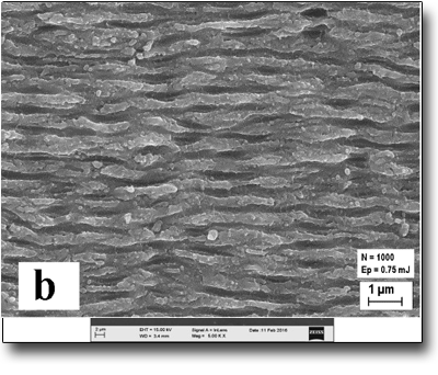
Enhanced selective solar absorption of surface nanotextured semi-insulating 6H-SiC
Optical Materials x (2020) xxxxxx
- Functional thin-films

Facilities
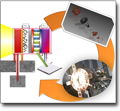
The activities and equipment of the DiaTHEMA Lab are organized into three facilities, dedicated for the synthesis of materials, for characterization of materials and devices, and for prototyping. The facilities are also supported by the mechanical workshop service.
- Facility for Synthesis of Materials
The thin-film materials’ deposition and processing facility is characterized by a wide choice of possible techniques that ensures great versatility in deposition, ranging from the growth of thin and ultra-thin films to the growth of polycrystalline structures. The main instruments include:
Two CVD reactors. Microwave enhanced CVD and Hot-filament CVD , typically used for the growth of synthetic diamonds;
An Electron beam evaporation system dedicated to the growth of thin and ultrathin films and for low electron affinity coatings;
A pulsed laser deposition system ns-PLD (@193 nm) that can operate in a reactive gas environment;
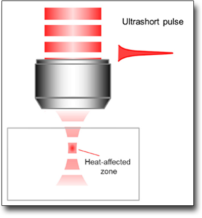
A uFAB - Micro & Nano processing laser materials fabrication workstation for nano- and micro-machining, shared with the FemtoLAB in Tito Scalo.
- Characterization facility
The characterization of materials and devices exploits the use and development of measurement techniques for morphological, optical, electronic, thermal and optoelectronic properties. All the experimental setups have been suitably optimized for the study of the performance and durability of advanced materials, both bulk and thin film form.
The main instruments supplied to the laboratory include:-
Atomic Force Microscope (AFM) AFM Quesant
-
Optical bench for Spectral photoconductivity composed by
-
High vacuum systems (10-8 mbar) VTEC
-
Solar simulator Solar furnace
-
Seebeck coefficient characterization system SEEBECK
-
Scanning Probe Microscopy SPM@DiaTHEMA
-
Infrared Thermo-camera for temperature measurements up to 2000 °C.
-
X-ray photoconductivity setup developed in collaboration with CNR-IC.
-
-
- Prototyping facility
Main instruments include:
-
A RF/DC magnetron sputtering deposition system Leybold LH Z400
-
An electron beam evaporation system, for metallization or the fabrication of multilayer devicesIONVAC EVPK 500EBK
-
A Reactive Ion Etching system for micromachining RIE
-
A Pulsed Laser deposition system (PLD) ns-PLD (@193 nm)
-
A mask aligner Photolitography 1µm
-
A thermal/ultrasonic microwire-bonding Kulicke & Soffa 4123
-
A femtosecond laser microfabrication workstation 2 Photon lithography
-
Collaborations
- Ionvac Process;
- Università la Sapienza;
- Solaris Photonics;
- Enea;
- Abengoa Research;
- Fraunhofer ISE;
- Tel Aviv University;
- Exergy;
- Technion - Israel Institute of Technology;
- Sharp;
- Prysmian;
- Alta;
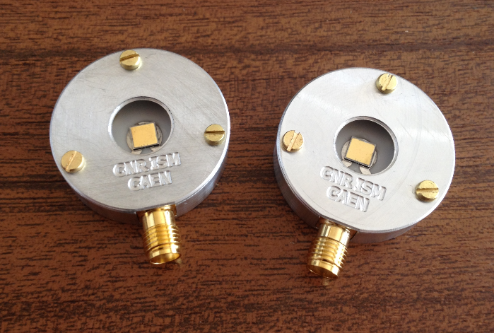
- CAEN;
- Università Roma Tre;
- INFN;
- Tübitak;
- Instituto de Energía Solar Universidad Politécnica de Madrid;
- Center for research and Technology Hellas Chemical Process & Energy Resources Institute
- Università degli Studi Niccolò Cusano
 Italiano (Italia)
  English (UK)