Since the late 1980s, ISM has developed activities and skills regarding the deposition and growth for Physical Vapor Deposition of superconducting, semiconductor, magnetic, and ceramic thin films that are of interest for electronics, sensors, optoelectronics, data storage, ICT and biomedicine applications.
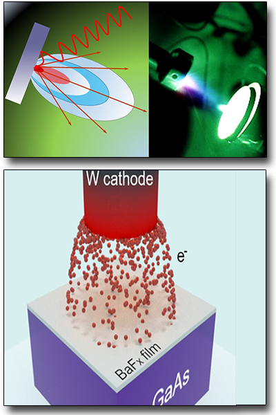
The techniques used range from thermal evaporation and RF-Sputtering to Laser Ablation and Deposition (Pulsed Laser Deposition - PLD). Thanks to the numerous laser sources available and the consolidated experiences acquired over the years by the ISM researchers, PLD represents a technique that can be used in different operating conditions, regulated by both the wavelength of the laser beam and the duration of its pulse as well as by the surrounding environment, that is the presence of: a background gas, a reactive atmosphere or high vacuum. For instance, this technique, whose laser-matter interaction processes and, for sufficiently long pulses (e.g. ns) also those interactions occurring between the laser induced plasma and the laser itself, are strongly dependent on the laser parameters used. The process is based on the "vaporization", in the form of plasma and even nanoparticles when ultrashort pulses, that is in the range of tens of fs are used. PLD can be applied to any inorganic, organic or biological material (e.g. oxides, carbides, nitrides, metals, alloys, polymers, biological materials, etc.) whose subsequent deposition on a support (substrate) is characterized by a complex control of the stoichiometric ratios and properties and dynamics of the various species involved making the laser source parameters and experimental conditions used the key factors for the deposited materials’ features. It follows that the deposition onto the surface of suitable and properly chosen substrates of the vaporized species provide the growth of innovative thin films, or new nanostructured materials. These can be obtained in either as a single or multilayer form or also, when in combination with other techniques such as RF-Sputtering, in order to deposit heterostructure that are otherwise difficult to be grown. ISM has five laboratories employing state-of-the-art PLD which are located at both its Roman branches of Tor Vergata and Montelibretti and at the Southern Italy branch of Tito Scalo (PZ). Because of the different experimental configurations available, the PLD typology to be employed can be chosen on both the laser source features (e.g. pulse duration: 120fs - 30ns, and wavelengths which spans from UV to NIR spectrum interval) or even in case other co-deposition systems or in-situ treatments are required (i.e. occurrind in the same deposition and growth chamber where the thin films or nanostructured materials under study are generated). To complete the variety of the PVD technique features offered, an electron beam evaporation system, valuable for the development of ultra-thin layers of fluorides, nitrides, carbides and borides, it is also available.
ns-PLD (@532 nm) ns-PLD (@193 nm) ns-PLD (@248 nm) ns-PLD (@1064-532-355-266 nm) Electron beam evaporator fs-PLD (@800-400 nm) Leybold-Heraeus Low Vacuum Evaporator
 English (UK)
  Italiano (Italia)