ns-PLD (@ 1064-532-355-266 nm) in HV or gaseous atmosphere, RF sputtering and thermal evaporation
Antonio Di Trolio -
Laboratory PLD and RF sputtering
TECHNICAL SPECIFICATIONS
-
PLD
-
Nd:Yag laser @1064 nm (higher harmonics: 532, 355, and 266 nm); 8-10 ns; Energy (mJ/p) = 850 (@1064 nm)(Spectra Physik, Lab 170)
-
UHV cylindrical deposition chamber with a top flange used as a viewport and with six lateral flanges. It's equipped with a multi-target carousel (up to 5) and a substrate heater that allow the deposition of films and multilayers up to 1000 C.
RF sputtering
-
1 "CF40 magnetron sputtering source (AJA INT mod. A310 XP)
-
automated matching network (SEREN IPS)
-
300 W RF power supply (SEREN IPS, mod. R301)
Thermal evaporation
-
HV chamber (10-7 mbar)
-
two thermal evaporation sources with quartz microbalance for thickness control (Inficon)
AVAILABLE TECHNIQUES
PLD of thin films of complex materials
- in-axis growth
- off-axis growth at variable angle between the axis of the plume and the normal to substrate
- reactive growth with O 2 , N2 gas
- growth of multilayers of different materials (up to 5)
- Real-time monitoring of temperature and growth by in-situ pyrometry
Sputtering deposition of thin films
- growth of conductive materials
- growth of insulating materials and semiconductors
- reactive growth with O2 , N2 gas
thermal evaporation of
- metallic films
- metal nanoparticles
SAMPLES
-
substrates with lateral dimensions: 10x10 mm (ideal), 3x3 mm (minimum), 15x15 mm or circular up to 25mm in diameter (maximum)
-
substrate thickness up to 1mm
-
film thicknesses up to 1 micron
USED FOR
- optoelectronics/spintronics
- solar/photovoltaic energy
CASE STUDIES
Ferromagnetism and conductivity enhancement in hydrogen irradiated Co-doped ZnO thin films grown by Pulsed Laser Deposition
ns-PLD (@ 1064-532-355-266 nm) in HV or gaseous atmosphere, RF sputtering and thermal evaporation
Antonio Di Trolio –
Laboratory PLD and RF sputtering
Rome – Tor Vergata
Fig._0_di_2_1_3
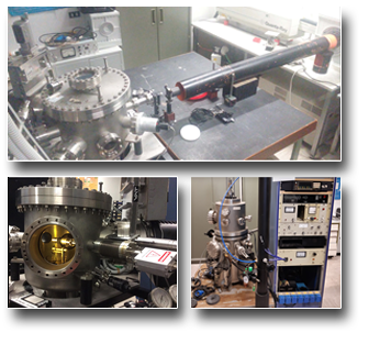
Physical vapor deposition (PVD) refers to a variety of high vacuum thin film growth techniques based on the vaporization of material from a solid source and subsequent condensation onto a substrate. This techniques allow to grow metal films, alloys, oxides, nitrides and composite materials on different substrates with thicknesses ranging from the nanometer to the micron scale. Pulsed Laser Deposition (PLD), sputtering deposition and thermal evaporation belong to this category. PLD is a versatile technique for the deposition of thin films of complex materials starting from a single target. A pulsed and focused high power laser beam is used to ablate material
from the surface of a target. The laser-matter interaction generates a plasma plume, containing atoms, ions and molecules, which expands in vacuum towards a substrate where nucleation and film growth take place. The stoichiometry transfer between target and film and the possibility of working in the presence of inert and reactive gas atmospheres up to pressures in the mbar range make PLD a very attractive technique.
Sputtering is also used for the deposition of thin films. The ions from a generated gaseous plasma are accelerated towards a target causing the emission of atoms and molecules. These neutral particles will travel in a straight line towards a substrate.
TECHNICAL SPECIFICATIONS
PLD
* Nd: Yag laser @ 1064 nm (higher harmonics: 532, 355, and 266 nm); 8-10 ns; Energy (mJ / p) = 850 (@ 1064 nm)
(Spectra Physik, Lab 170)
* UHV cylindrical deposition chamber with a top flange used as a viewport and with six lateral flanges. It's equipped with a multi-target carousel (up to 5) and a substrate heater that allow the deposition of films and multilayers up to 1000 C.
RF sputtering
* 1 "CF40 magnetron sputtering source (AJA INT mod. A310 XP)
* automated matching network (SEREN IPS)
* 300 W RF power supply (SEREN IPS, mod. R301)
Thermal evaporation
* HV chamber (10-7 mbar)
* two thermal evaporation sources with quartz microbalance for thickness control (Inficon)
AVAILABLE TECHNIQUES
PLD of thin films of complex materials
* in-axis growth
* off-axis growth at variable angle between the axis of the plume and the normal to substrate
* reactive growth with O2, N2 gas
* growth of multilayers of different materials (up to 5)
* Real-time monitoring of temperature and growth by in-situ pyrometry
Sputtering deposition of thin films
* growth of conductive materials
* growth of insulating materials and semiconductors
* reactive growth with O2 and N2 gas
thermal evaporation of
* metallic films
* metal nanoparticles
SAMPLES
* substrates with lateral dimensions: 10x10 mm (ideal), 3x3 mm (minimum), 15x15 mm or circular up to 25mm in diameter (maximum)
* substrate thickness up to 1mm
* film thicknesses up to 1 micron
USED ??FOR
* optoelectronics/spintronics
* solar/photovoltaic energy
CASE STUDIES
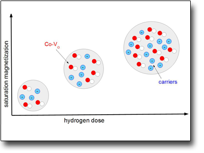
Ferromagnetism and conductivity enhancement in hydrogen irradiated Co-doped ZnO thin films grown by Pulsed Laser Deposition
Co-doped ZnO thin films were grown by pulsed laser deposition on single crystal sapphire substrates. Post-growth hydrogen irradiation at temperatures of 400 °C promotes hydrogen incorporation which increases the saturation magnetization and the carrier density.
See: A. Di Trolio et al. et al., ACS Appl. Mater. Interfaces 2016, 8, 12925
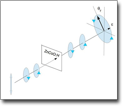
Giant magneto-optical effect in H-irradiated Co-doped ZnO thin films grown by pulsed laser deposition+
Remarkable improvements in the magneto-optical properties of Co-doped ZnO thin films were achieved by post-growth hydrogen irradiation. A giant Faraday rotation of 3000 deg/cm was observed at 400 nm. Optical, structural and microstructural characterizations show the full Zn substitution by Co, ruling out the presence of noticeable Co-related secondary phases down to the nanoscale.
See: DOI:10.1039/C8TC03563F
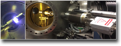
Reduction of secondary electron emission in carbon films grown on copper by RF magnetron sputtering
Carbon films grown on copper by RF magnetron sputtering showed a decrease of the secondary electron emission (SEY) following a graphitization process through thermal annealing. XPS, Raman and SEY measurements show the structural reorganization of amorphous C in nanocrystalline graphite and the reduction of SEY.
See: R. Larciprete et al., Applied Surface Science 328 (2015) 356-360
 English (UK)
  Italiano (Italia)