TECHNICAL SPECIFICATIONS
- Spectra Physics Ti:Sa “fs” Laser
Spitfire Pro - Regenerative Amplifier (120 fs; 1kHz; 4 mJ @ 800 nm; SH: 1.5 mJ @ 400 nm) - Quanta System Nd:YAG “ns” Laser
Prototype (7 ns; 10 Hz; 100 mJ @ 532 nm) - Time-resolved spectroscopy and imaging
- Andor iStar “Inductively Charge Couple Device – ICCD” camera (t ≥ 2 ns; Spectral range = 250-900 nm, Pixeldim = 13 μm x 13 μm)
- ARC SpectraPro 300i monochromator (Spectral range = 200-1000 nm; ʎ/Δʎ = 10000)
- Vacuum chamber
- pmin = 10-7 mbar;
- Tmax (substrate holder) = 800 °C
AVAILABLE TECHNIQUES
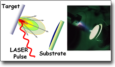
- Deposition at RT or high temperature (eg. (max 800°C) in HV or controlled gaseous environment (es. Ar, N2, He, O2) of various kind thin films and nanostructured inorganic materials:
- Carbides, oxides, nitrides, borides, etc.
- Noble metals (e.g. for plasmonic applications)
- The PLD activities are also carried out in collaboration with the Physical-Chemistry Laser Laboratory of the University of Basilicata which expands the offer by the availability of other experimental equipments and techniques for characterizing the obtained deposits (e.g. HR-TEM).
SAMPLES
- Solid and flat samples with side dimensions 10 mm x 10 mm (minimum) and 25 mm x 25 mm (maximum); thickness 20 mm (maximum).
USED FOR
-
Optoelectronics
-
Optical components
-
Thermoelectric devices
-
Tribological coatings
-
Magnetic devices
-
Semiconductors
-
Microbattery electrodes
-
Biosensors
-
Biocompatible coatings
-
Plasmonic systems
-
Superconductors
-
Thermionic systems
CASE STUDIES
Features of the NPs deposited by fs-PLD
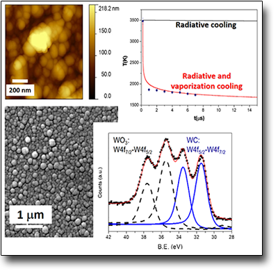
The laser ablation and deposition performed by fs pulses allows the direct deposition of NPs:
* having an initial temperature of approximately 3500 K which decays exponentially over time;
* that during their flight towards the substrate onto which they deposit, a variation of their stoichiometry can take place as a consequence of a differential evaporative cooling of the involved species;
* form nanostructured deposits which, compared to the starting target, may miss part of the most volatile components;
* whose initial dimensions are centered around 5-10 nm giving rise, for long deposition times, to agglomerations having dimensions up to a few hundred nm
* which can give crystalline structures by increasing the substrate temperature although, however, it can affect to a further stoichiometry variation of the final deposit.
See: Angela, De Bonis et al. Appl. Surf. Sci. 258, 9198 (2012)
DOI: 10.1016/j.apsusc.2011.07.077


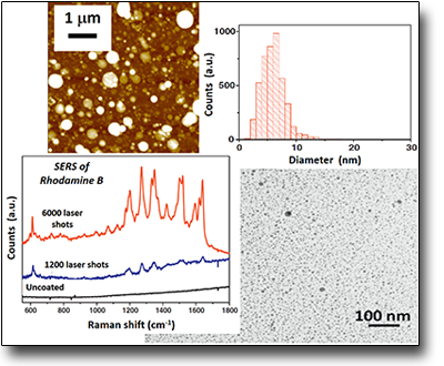
Deposition of Ag nanoparticles for SERS applications
The direct deposition of NPs by fs-PLD is immediately exploitable for getting nanostructured films which can be extremely beneficial for several applications. For instance, by fs-PLD of Ag, it has been demonstrated how the surfaces obtained, due to their localized surface plasmon resonance (LSPR) properties, are straightforward operating efficiently for enhancing the electromagnetic Raman scattering for the Surface Enhanced Raman Scattering (SERS) technique, whose signal amplification effect can exceed ten orders of magnitude.
See: Angela, De Bonis et al. Surf. Coat. Tech. 207, 279 (2012)
DOI: 10.1016/j.surfcoat.2012.06.084
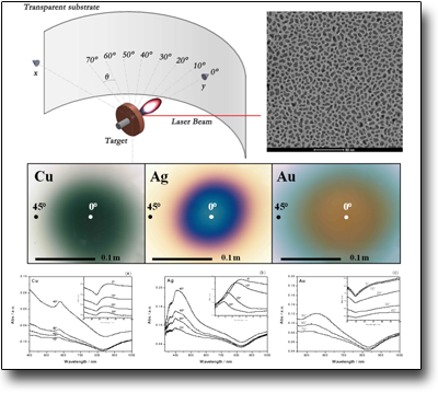
Plasmonic angular tunability of Cu, Ag and Au nanoparticles generated by fs PLD
Noble metals NPs’ angular distribution induced by fs PLD plays a relevant role in providing spatially resolved NPs distribution on top of substrates and characterizing the resulting thin films' properties. As demonstrated by our published study, different grade of Au NPs’ agglomeration follows the NPs’ angular distribution which leads to spatially resolved plasmonic tunability of the obtained deposits offering new perspectives for their application in several fields such as biosensors and optoelectronic devices.
See: Maria Lucia, Pace et al., Appl. Surf. Sci. 374, 397 (2016)
DOI:10.1016/j.apsusc.2016.02.111
Contatto: Ambra Guarnaccio -


 English (UK)
  Italiano (Italia)