TECHNICAL SPECIFICATIONS
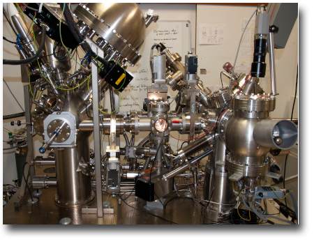
Omicron system consisting of four main chambers
- Fast-entry lock (FEL)
- Sample introduction
- 5 gas distribution lines
- Transfer chamber
- Sample exchange between FEL, PC and AC
- Sample exchange between FEL, PC and AC
- Preparation chamber (PC)
- Sample cleaning, preparation and inspection
- Ion gun for sputtering (Ar+) with energy 0.8–5000 keV
- 4-axis manipulator
- Two heating stages: (i) resistive (RT–500 °C), (ii) e-beam (RT–900 °C)
- Two ports for evaporators (CF40) with differential pumping
- Quartz crystal microbalance (QCM) as thickness monitor
- RT-STM
- LEED
- Quadrupole mass spectrometer (detection range 0–100 m/q)
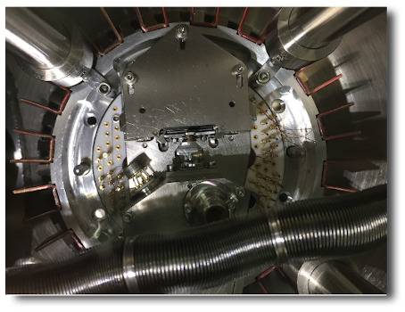
- Analysis chamber (AC)
- X-ray source with twin anode (Al, Mg)
- Monochromated X-ray source (Al)
- UV source (HeI, HeII)
- EA125 electron analyzer (5 channeltrons)
- 5-axis manipulator with resistive heating stage and motorized azimuthal and polar angle movements
AVAILABLE TECHNIQUES
- X-ray photoelectron spectroscopy (XPS), Twin anode + Monochromated X-rays
- X-ray photoelectron diffraction (XPD)
- UV photoelectron spectroscopy (UPS)
- Angular-resolved photoelectron spectroscopy (ARPES)
- Low-energy electron diffraction (LEED)
- Room temperature scanning tunneling microscopy (RT-STM)
- Mass spectrometry (MS)
SAMPLES
-
Samples are mounted on flag-style Omicron sample plates
-
Maximum allowed sample lateral size: 10 mm (diameter) or 8×8 mm2
-
Maximum allowed sample thickness: 3 mm
-
Sufficient conductivity to avoid charging during photoemission experiments and ensure stable tunneling current in STM
USED FOR
-
Metals
-
Semiconducting samples
-
Thin films
-
Single crystals and polycristals
TECHNIQUES AVAILABLE FOR PREPARATION/CLEANING
- Ar+ ion sputtering with energy 0.8–5000 keV
- Annealing (RT–900 °C)
- Exfoliation of layered samples in vacuum
- Evaporator for organics
- Thickness monitor
CASE STUDIES
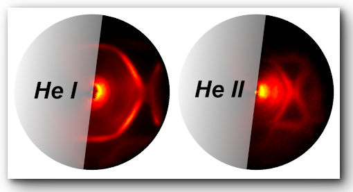
ARPES - Fermi surface maps
Our experimental setup allows the measurement of angle-resolved UPS data. Depending on the specific case, one can acquire full-3D ARPES plots (kx e ky vs E), carpet plots (kx vs E) o or angular maps (kx e ky) at fixed energy. We report here an example of the latter acquisition mode, where the Fermi surface of a clean Au(111) surface has been mapped using He I and He II as photon sources.
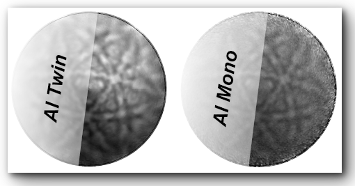
XPD angular plots display the angle-resolved photoelectron intensities from a particular emission line. At electron energies above ~500 eV, the scattering intensity is mostly directed in the forward direction, enhancing the photoelectron flux along the emitter–scatterer axis (forward-focusing effect). This method provides insights into the structure of surfaces and adsorbates. Here, we measured the XPD plot of a clean Au(111) sample at the Au 4f7/2core level, with both twin and monochromated X-ray sources.
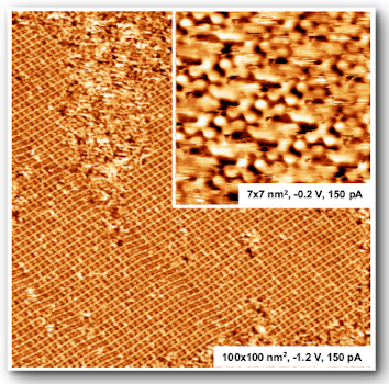
Molecular self-assembly
One of the core activities carried out in our laboratory is the study of molecular systems on surfaces. The growth of covalent nanostructures can feature the appearance of intermediate phases. Here, we report the STM image of the Au(111) surface covered with a self-assembled phase of molecular dimers. The packing of the organic units into stable islands allows the identification of each molecule with high resolution. Image acquired at room temperature with an etched tungsten tip.
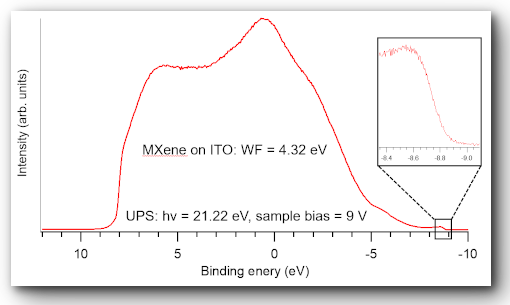
UPS measurements of samples that are biased allows the determination of the surface work function. Here, an ITO substrate was used to deposit a layer of MXenes. UPS measurements with the He I photon source of a 9 V biased sample revealed its work function of 4.32 eV.
 English (UK)
  Italiano (Italia)