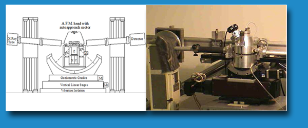
ED X -ray reflectometer with integrated AFM
Barbara Paci -
TECHNICAL SPECIFICATIONS
- Siefert 3.5KW Generator: typical working conditions E=55 kV, I=40 mA max.
- X-Ray sources with W and Ag anode
- ORTEC Ge-Single crystal solid state detector
- ORTEC-ADCAM Electronic data acquisition
- In House acquisition software
- Motorized arms, max 32°for each arm
- W collimation slits (square or rectangular collimation) : max collimation 20*20 μm
- Step-motor cradle
- Continuous double axis cradle
- Manual and motorized translators (x-y)
- Standard sample holder, especially designed sample holders for controlled atmosphere and thermal treatments up to 200°C max.
- Integrated AFM sample holder
AVAILABLE TECHNIQUES
- Classical EDXR
- In-situ EDXR
- Time-resolved EDXR
- Joint EDXR/AFM
SAMPLE
-
FThin films: film thickness 40-3000Å; max sample thickness 3cm; max in plane dimensions 10cm*10cm..
-
Multilayered samples: max. thickness for each layer 40-3000Å; total sample thickness max 3cm; in plane max. dimensions 10cm*10cm.
-
Samples to be measured in controlled atmosphere or in temperature, max in plane dimensions 2cm*2cm.
USE FOR
- Determining morphological parameters as thickness and roughness of thin films/multilayers.
- Determining electron density of thin films/multilayers.
- In situ time resolved monitoring of morphological parameters evolution for thin films/multilayers as a function of external conditions: ambient conditions, controlled atmospheres, polluting gasses, thermal treatments, light exposure.
- In situ time resolved electron density monitoring of thin films/multilayers as a function of external conditions: ambient conditions, controlled atmospheres, polluting gasses, thermal treatments, light exposure.
Case Studies
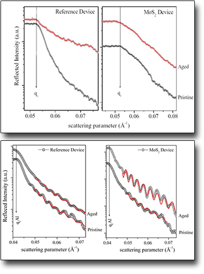
Extending the Continuous Operating Lifetime of Perovskite Solar Cells with a Molybdenum Disulfide Hole Extraction Interlayer.
Lead halide perovskite solar cells are one of the most promising photovoltaic technologies. Here, it is shown how the introduction of MoS2 flakes as a hole transport interlayer significantly improved the stability of encapsulated devices Such effects ascribed to the twofold beneficial role of MoS2,inhibiting both interface and structural aging pathways, as demonstrated by XRD and EDXR experiments.
See: G.Kakavelakis, I.Paradisanos, B.Paci, et al. Adv. Energy Mater. 2018, 1702287
See news:
http://grafene.cnr.it/celle-solari-a-perovskite-piu-stabili-grazie-a-cristalli-bidimensionali/
https://www.cnr.it/it/news
See twitter:
https://twitter.com/graphenefactory/status/1005019272559693826

Conductivity via Thermally Induced Gap States in a Polyoxometalate Thin Layer.
Polyoxometalates are as an emerging class of materials in organic optoelectronics. X-ray reflectivity is used for determination of layer thicknesses and scattering length densities: nanostriped films a few tens of nm thick can be obtained and that such structuring is accompanied by the appearance of gap states and by a switch from an insulating to a conductive state. Integrating the layer into an organic photovoltaic device the conduction through it thanks to favorable band alignment between ITO, the gap states, and the active photovoltaic layers.
See: Qirong Zhu, Barbara Paci et al. J. Phys. Chem. C 2019, 123, 1922−1930
 Italiano (Italia)
  English (UK)