The medium temperature stage is also configured to be illuminated by an external lighting source through a MgF2 window (transparent in the visible region), particularly suitable for the characterization of photon-enhanced thermionic emission (PETE) materials.
The VTEC's equipment is completed by a vast assortment of instruments useful for electrical characterization, such as picoammeters (HP4140B, Keithley 487), voltage and current sources (Keithley 6220), electrometers and source meters (Keithley 6517A, 617, 2440), nano- voltmeters (Keithley 2182), wave generators (Keithley 3390), impedance and phase analyzers (Solartron 1255, 1260, HP 4192A, HP 4275A).
TECHNICAL SPECIFICATION
-
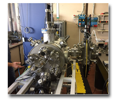
base pressure < 10-7 mbar;
-
3 heating stages at low (up to 600°C), medium (up to 1000 °C) and high temperature (up to 1800°C);
-
electrical characterization of samples as a function of temperature;
-
External illumination allowable in the medium temperature stage.
AVAILABLE TECHNIQUES
VTEC - Impedance spectroscopy
The impedance spectroscopy is a very useful tool to investigate the dielectric and transport properties of complex materials. The experimental objective is measuring the resistance, capacitance and inductance contributions provided by a material or device when a time-modulated electrical input is applied to it.
The electrical input applicable on the system can be:
-DC bias up to 20 V,
-AC bias signal can up to 1 V peak-to-peak,
-modulation frequency up to 20 MHz.
Measurements can be performed in the moderate temperature stage up to 600 °C.
VTEC - Four-point-in-line probe in T @ 600 °C
The four-point-in-line probe is a technique for deriving the layer resistance of a film and, if the thickness is known, its resistivity. The external points of the probe inject a given current, whereas the internal ones measure the voltage drop. In this way, any contact resistance and series resistance than the film is excluded from the measurement.
The electrical input bias is characterized by:
- Currents from pA to mA range;
- Measurable voltage drops from nV to 100 V,
- Maximum resistance of 108 Ω.
Measurements can be performed continuously up to the temperature of 250 °C and intermittently (the probe can be translated vertically) in the moderate temperature stage up to 600 °C.
VTEC - Van der Pauw electrical characterization @ RT
The Van der Pauw configuration is aimed at measuring the layer resistance of a film and differs from the collinear 4-in-line probe in the geometry, since it foresees a specular symmetry along the two directions in which the film plane lies. Such measurements are performed at room temperature in air.
VTEC - Thermoionic electron emission
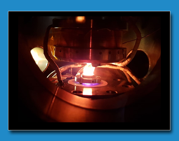
Thermionic emission measurements can be performed up to 1000 or 1800 °C, depending on the stage type, to characterize the electron emission capability of a material so to derive its work function and Richardson constant. Also the behavior of thermionic collectors can be characterized on a combined stage able to reach temperatures < 500 °C.
Full current-to-voltage characteristics can be obtained by adjusting the bias voltage from the retarding to the accelerating regime.
By illuminating the sample of the high temperature stage through a magnesium fluoride window or two optical fibers, it is possible to perform photon-enhanced thermionic emission measurements up to about 800 °C.
VTEC - Spectrally resolved total photoemission yield
The combination with a deuterium lamp and a monochromator allows the illumination of the moderate temperature stage with a radiation with a wavelength ranging from 190 to 550 nm.
A grid anode collects the emitted electrons, thus allowing estimate the emission quantum efficiency of the material, the work function value and the electron affinity in case of semiconductors.
SAMPLES
-
maximum lateral size:
-
20x20 mm2 (moderate temperature stage);
-
100 mm diameter (high temperature stage)
-
50 mm diameter (ultra-high temperature stage)
-
USE FOR
- wide bandgap semiconductors;
- III-V semiconductors;
- refractory metals;
- photovoltaic cells;
- hybrid thermionic-photovoltaic systems;
- photon-enhanced thermionic emission systems.
CASE STUDIES
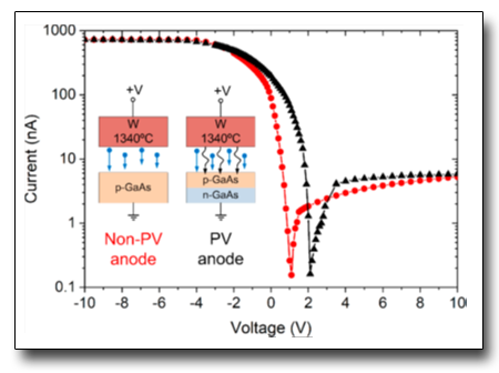
Photovoltaic Anodes for Enhanced Thermionic Energy Conversion
Ref.: A.Bellucci et al., ACS Energy Lett. 5 (2020) 1364-1370
 English (UK)
  Italiano (Italia)