TECHNICAL SPECIFICATIONS
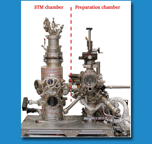
- Omicron LT-STM
- STM stage equipped with:
- 4-contacts option
- Superconductive coil, up to 400 Gauss (40 mT) ^ to sample surface
- Operating temperature:
- (300 ÷ 78) K with N2 liquid
- (78 ÷ 4.7) K with He liquid
- (4.7 ÷ 2.3) K with He liquid + cryostat pumping.
- P< 1×10⁻¹⁰ mbar
-
PREPARATION CHAMBER
- LEED/Auger optics
- Manipulator with resistive heater (max 800°C) and/or direct heating (max 1250 °C).
- Ion gun
- Knudsen cell
- Electron bombardment deposition system
- Quartz crystal microbalance
- Gas line (Ar, O2, H2, NH3, C2H2…)
- Mass spectrometer
- In vacuum tip cleaning system
- Cleaver for layered samples
- P< 5×10⁻¹⁰ mbar
AVAILABLE TECHNIQUES
-
Scanning tunneling microscopy (STM)
-
Scanning tunneling spectroscopy (STS)
-
Low energy Electron Diffraction (LEED)
-
Auger electron spectroscopy (AES)
TECHNIQUES AVAILABLE PREPARATION/CLEANING
-
Ion sputtering
-
Annealing
-
Layered samples cleaving
-
Chemical vapor deposition (CVD)
-
Monitoring of the deposited materials flux
-
Deposition of a wide range of organic molecules
SAMPLES
-
Sample lateral dimensions: max 10x10 mm2
-
Sample thickness: max 3 mm
-
Sufficient electrical conductivity to ensure stable tunneling current
-
In situ, sample preparation to be discussed with the staff
-
Mechanical integrity
USE FOR
- Metals
- semiconductors
- thin films.
Case Studies
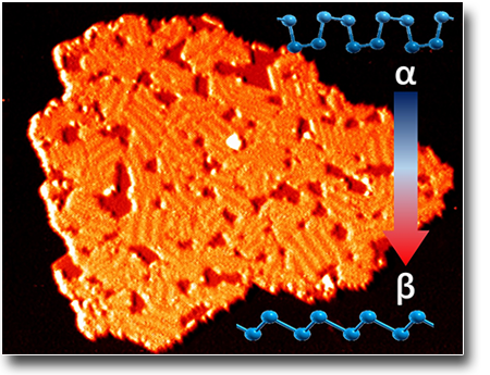
The two-dimensional allotrope of antimony, β-antimonene, defined as the buckled Sb analogue of graphene, has drawn the attention of the scientific community due to its peculiar electronic band structure which might be exploited in electronics, spintronics, optoelectronics and even thermal energy conversion.
In this study a method to induce the α to β phase transition of antimonene deposited on a Bi2Se3 crystal by means of annealing is investigated. The phase transition at the atomic scale is observed by scanning tunneling microscopy, while density functional theory calculations comprehensively explain why the α phase is energetically favored upon growth on Bi2Se3 at room temperature as well as why, and indeed how, the β phase forms upon gentle annealing.


ACS Nano submitted
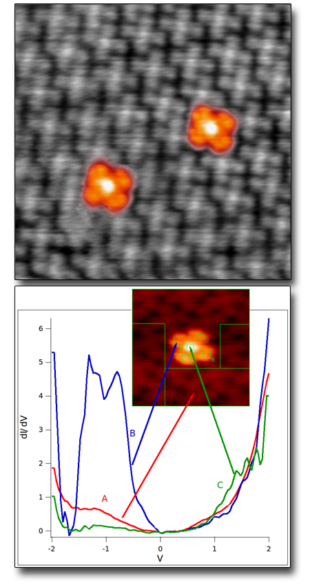
In the work here reported as a case study, using the tunneling microscopy, a detailed picture of the molecular orbitals rearrangement due to the contact with the substrate is drawn, elucidating how the work function of the substrate impacts the molecule spin pattern. Indeed, the tunneling microscopy allows to map the molecular orbitals density of states with a sub-molecular resolution. On the other hand, the tunneling spectroscopy measurements provide the energy distribution of these states. The data analysis of tunneling microscopy/spectroscopy is supported by theoretical modeling performed by the theory group at ISM.


 English (UK)
  Italiano (Italia)