Research Activities
NanoLab@ISM has a rich know-how in the field of synthesis and investigation of surfaces and interfaces produced through a wide range of physical deposition techniques. The conducted studies are always of a basic research nature, however, they concern materials and structures of technological significance. The scientific interest is mainly addressed to the structure of the surfaces and interfaces at the atomic level, to the electronic properties deriving from this atomic structure, to the topological properties of the materials (in particular at the surface) and to all those properties emerging from the formation of the interface. The investigation tools used in these studies are tunneling microscopy and spectroscopy (STM/STS), low energy electron diffraction (LEED), Auger spectroscopy (AES) and spectroscopy techniques based on synchrotron radiation (photoemission, absorption). Moreover, the NanoLab@ISM group possess skills in ultra-high vacuum (UHV) technology and in the physical deposition techniques of materials for the formation of controlled inorganic and hybrid organic/inorganic interfaces. The analysis of the experimental results is carried out with the aid of first principle modeling methods in collaboration with the ISM theory group.
The laboratory has always been open to collaborations at various levels and carries out didactic activities proposing degree theses and laboratory stages.
While maintaining a strong intersectoral character, the research activity at NanoLab @ ISM can be roughly divided into three macro lines: 2D materials; nanostructures; interfaces.
2D Materials
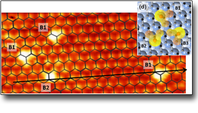
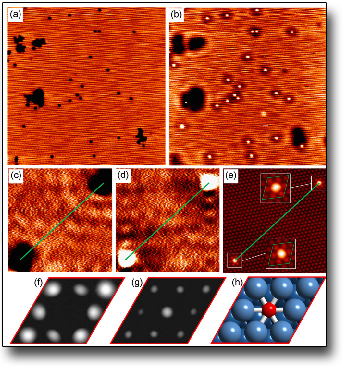
The research on 2D materials is a wide field crossing the basic and applied research. The activity of our group in this sector is oriented to the development of physical deposition methods for 2D materials, graphene and beyond graphene, to the comprehension of the material interaction with the substrate and to the electronic properties deriving from this interaction. Moreover, taking advantage from the high spatial resolution of the scanning tunneling microscope, the effects of local deformations on the electronic structure of the 2D material are investigated. Below examples of works on 2D materials are reported illustrative of the NanoLab@ISM activity.
Nanostructures
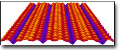
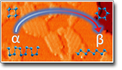
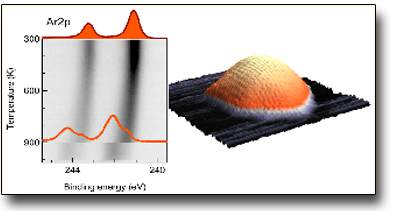
Our research activity is oriented to the study of self-assembled nanostructures on different substrates. These nanostructures are produced following a bottom-up approach by using physical techniques in ultra-high vacuum conditions. The configuration and size of the structures produced with these techniques are influenced by the interaction with the substrate. The structural and electronic properties of these nanoparticles are investigated with microscopy and spectroscopy techniques. Below are reported two examples of how it is possible to control the organization of these structures by using appropriate substrates.
Interfaces
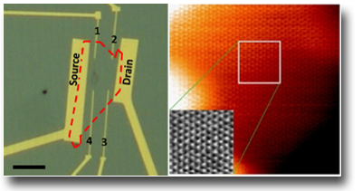
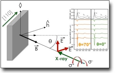
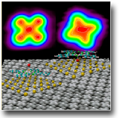
The study of the interfaces is of paramount interest in a lot of technology sectors. Our research in this field deals with the phenomena leading to the interface self-assembling, the charge transfer phenomena at the interface and the electronic and magnetic properties. In particular our interest is devoted to hybrid organic/inorganic, metal/semiconductor and Si(111)/β-Si3N4 Interfaces. The examples reported below show the different properties studied: structural; electronic; magnetic.
Instrumentation
Collaborations
- Dipartimento di Fisica Università degli Studi di Roma Tor Vergata
- Dipartimento di Fisica Università degli Studi di Roma La Sapienza
- Istituto Nanoscienze-CNR, Pisa
- Istituto dei Sistemi Complessi-CNR, Roma
- Dipartimento di Fisica Università di Camerino
- CNRS - CINaM Marsiglia, Francia

 English (UK)
  Italiano (Italia)