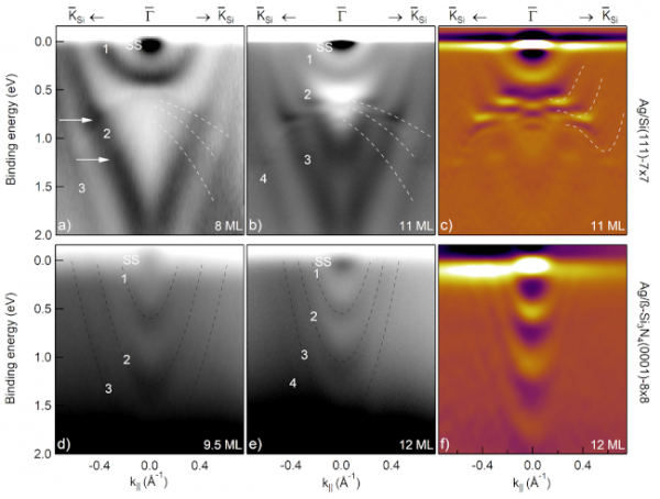
We have observed quantum well states on the Ag/Si(111) and Ag/β-Si3N4/Si(111) interfaces, by angle-resolved photoemission spectroscopy. This has been made it possible by the two-step growth technique, where silver is first deposited at low temperature and then is left recovering RT. The data display the full confinement of the electrons in the nitride gap for the Ag/β-Si3N4/Si(111) interface, at variance with the case of Ag/Si(111), where the QW states partially resonate with the continuum of the bulk silicon bands. Therefore, the nitride layer, although very thin (less than 1 nm), restores the vertical potential wall towards the highly n-doped silicon substrate, so that silver can show the valence electronic structure of a nearly free-standing layer.
Tuesday, 07 September 2021 09:27
Effect of a subnanometer thin insulator layer at the Ag/Si(111) interface through the observation of quantum well states
 Comparison between the electronic structure of the Ag / Si and Ag / Si3N4 / Si interface (high and low, respectively). The quantum holes in the case of the presence of nitride show the absence of interaction between the valence states of silver and silicon.
In this paper published on Physical Review Materials, the “two-step” growth technique has been used to grow atomically uniform Ag films on 7×7 Si(111) and 8×8 β-Si3N4(0001)/Si(111) surfaces. Angle-resolved photoemission spectroscopy reveals the formation of sp quantum well states in the Ag films with distinct properties in the two cases. It is shown that the valence electrons in silver can be confined in the fundamental gap of a less than 1-nm-thin nitride layer, effectively decoupling the Ag and Si states.
#electronic_structure #quantum_interference_effects #surface_reconstruction #surface_states
Published in
Publications

 English (UK)
  Italiano (Italia)