Research Activities
The team research program is focused on the study of functional materials for applications in fields such as optoelectronics, spintronics and solar energy. The Laboratory activity is mainly dedicated to the growth of thin films of semiconductor, superconducting, semi-metallic, perovskite oxides by physical vapor deposition techniques (PVD) and study of structural, electrical, optical and magnetic transport properties.
Wide gap semiconductors
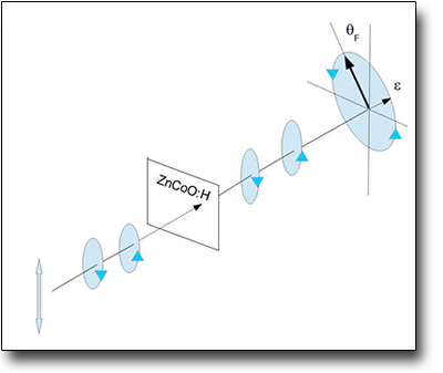
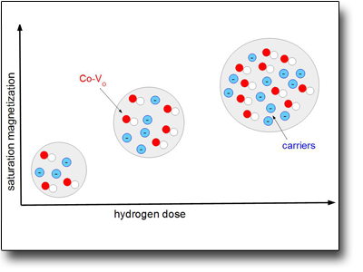
It is a class of semiconductor materials characterized by a 2-4 eV bandgap, larger than that of conventional semiconductors (i.e silicon, with Eg=1-1.5 eV). Thanks to their high optical transparency together the possibility of electrical conductivity modulation by proper doping, they are key materials for optoelectronic devices and enregy applications. The team’s research activity is devoted to the growth and study of transparent and conductive oxides (TCO), obtained by doping semiconductor materials (ZnO, TiO2) with donor ions (Al, Ga) and diluted magnetic semiconductors (DMS), obtained by doping with transition metal ions (Co, Mn).
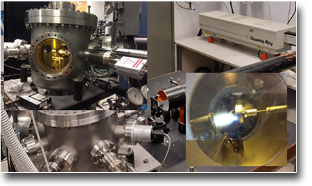
Instrumentation
Collaborations
- University La Sapienza, Physics Department
- University of Salerno, Physics Department
- Universita of Rome Tor vergata, Engineering Department
- CNR- SPIN
- INFN, national laboratories of Frascati
 Italiano (Italia)
  English (UK)