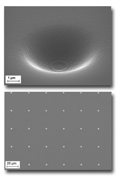
Two optical lithography techniques are available: 1) Ultraviolet lithography also known as photolithography, which is the most common used patterning technique in microfabrication, 2) 2-photon lithography, which is a high resolution 2D and 3D structuring process of a photosensitive material induced by an ultrashort pulse laser with radiation intensity sufficiently over a defined threshold.
In the case of photolithography, the photoresist (a photosensitive material) is spin-coated onto a substrate and illuminated with UV light through a photomask containing the geometric patterns. After the required exposition and development of the sample, the desired pattern is transferred on the photoresist. DiaTHEMA Lab of ISM, located in the Montelibretti Section, has a setup composed by a Karl Süss MA6 mask aligner, able to reach a resolution of about 1 μm, and a SUSS MicroTec LabSpin spin coater, with maximum speed of 5000 rpm. The setup is mounted in a clean room to improve the cleanliness of lithography process. It is possible to use both positive and negative photoresist, with thickness up to 30 μm.
In case of 2-photon lithography, 2D or 3D mask-less patterns can be obtained by direct-writing with the ultrashort-pulse laser beam, that can be focused down to the sub-micrometer resolution. Features of a few hundreds of nanometers are achievable thanks to the existence of intensity threshold, which allow pushing the resolution over the laser spot size. The setup consists of the Ti:sapphire femtosecond laser (pulse length of about 100 fs) and the nanoresolution workstation Newport MicroFab, located in the Tito Scalo Section and managed by FemtoLAB and DiaTHEMA Lab.


 English (UK)
  Italiano (Italia)