Further information at: http://www.elettra.eu/elettra-beamlines/vuv.html
TECHNICAL SPECIFICATIONS
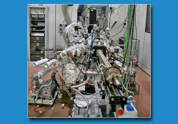
Beamline
- Photon energy: 20-750 eV.
- Resolving power: 20000 at 65 eV, 14000 at 400 eV.
- Light polarization: horizontal.
- Measurement chamber
- Base pressure: 5 × 10-11 mbar.
- Sample temperature: 9 - 450 K.
- Degrees of freedom of the manipulator: 5.
- Energy and angle resolution of the electron spectrometer: 2 meV (at 5 eV pass energy) and 0.1°.
Preparation chamber
- Base pressure: 1 × 10⁻¹⁰ mbar (up to 10-6 mbar during controlled exposure to pure gases) mbar.
- Sample temperature: 77 - 1000 K (liquid nitrogen cooling and electron beam annealing).
- Degrees of freedom of the manipulator: 5.
Heating chamber
- Base pressure: 5 × 10⁻⁹ mbar -10 mbar (up to 10-3 mbar during controlled exposure to pure gases).
- Sample temperature: 300 - 2000 K (electron beam annealing).
- Sample parking stage
- Magnetization coil
AVAILABLE TECHNIQUES
Measurement chamber
- Angle-resolved photoemission spectroscopy (ARPES) for valence band and Fermi surface mapping.
- High-resolution X-ray photoemission spectroscopy of core levels (XPS).
- X-ray photoelectron diffraction (XPD).
- X-ray absorption spectroscopy (XAS).
- Residual gas analysis (RGA).
Preparation chamber
- Low-energy electron diffraction (LEED).
- Molecular beam epitaxy (MBE) controlled by a quartz micro-balance.
- Ion sputtering.
- Residual gas analysis (RGA).
Heating chamber
- Chemical vapor deposition (CVD).
SAMPLES
-
The electrical conductivity of the samples must be high enough to avoid charging effects.
-
Metals, small gap semiconductors and ultra-thin insulating films are usually suitable materials for the analysis by photoemission spectroscopy.
-
Lateral size: from 2 × 2 to 10 × 10 mm22.
-
Thickness: up to 2 mm.
USED FOR
Study of the electronic and magnetic structure of:
-
2D materials (e.g. graphene, silicene, antimonene);
-
topological matter (topological insulators, Weyl semi-metals);
-
low-dimensional systems with high spin-orbit coupling and/or magnetic interactions;
-
self-assembled molecular layers.
Case Studies
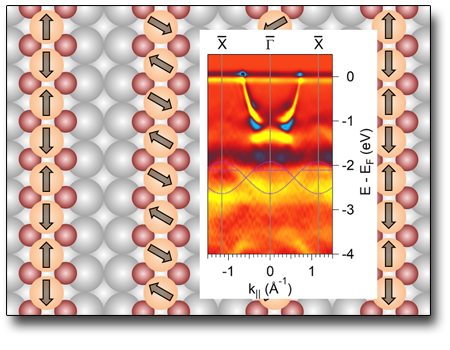
Indirect chiral magnetic exchange through Dzyaloshinskii–Moriya-enhanced RKKY interactions in manganese oxide chains on Ir(100)
Manganese oxide chains grown on Ir(100) display a non-collinear spiral magnetic structure, which has been identified by spin-polarized scanning tunneling microscopy and theory. ARPES spectra show the effects on the Mn 3d states of the anti-ferromagnetic ordering along the chains, where the Mn atoms are adjacent.
See: M. Schmitt et al., Nat. Commun. 10, 2610 (2019)
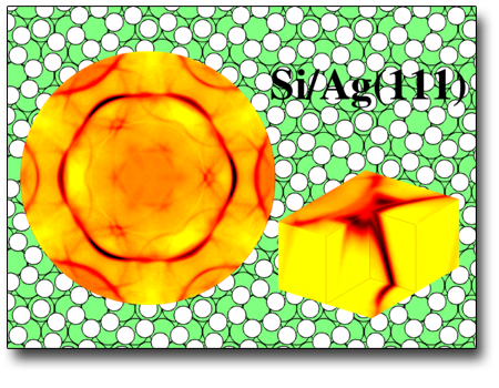
Electronic States of Silicene Allotropes on Ag(111)
Silicene is a honeycomb-like material similar to graphene and consisting of a single layer of silicon atoms. Some silicene allotropes can be synthesized on Ag(111). The ARPES analysis shows that these allotropic forms present σ-derived bands, while the π-derived bands expected in the proximity of the Fermi level are fully de-localized in Ag the substrate. This hybridization does not allow the formation of Dirac cones, at variance with the case of free-standing silicene.
See: P.M. Sheverdyaeva et al., ACS Nano 11, 975 (2017).
 English (UK)
  Italiano (Italia)