III-V MBE 2 growth system MBE2 (III-V)
Paola De Padova -
Carlo Ottaviani -
Sandro Priori -
Laboratory IC11
In epitaxy the surface is exposed to a gas, for example, Metal (M)/Semiconductor (SC) vapor, which condenses on the surface. In this way the surface becomes a contact place between two solids which is called: interface. The fundamental question in epitaxy is whether the gas atoms adsorbed on the surface wet the surface or form islands. This case occurs as a result of strong forces between adsorbate and surface atoms (at T=0): this is a typical case of adhesion. If the adsorbate-adsorbate interaction is stronger than adsorbate-surface interactions, islands form on the surface, which are termed clusters. Hence, the wetting properties of a “gas” upon a specify surface are the necessary conditions for the epitaxial growth.
TECHNICAL SPECIFICATIONS
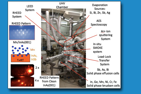
- Working pressure ~10-10 mbar mbar
- In, Ge, Mn, Ni, Cr, Fe effusion cells;
- Sb, As, Bi- Surfactants effusion cells;
- Ag, Zn- Capping Layer effusion cells;
- DC direct sample heating (RT-1200 °C) and Indirect heating (RT-450 °C ) systems
- Air-vacuum Fast Load-lock Sample Transfer System;
- Quartz Microbalance;
- Ar+ Ion sputtering system;+;
- O Gas-line;
- e-- HV variable (0-15) KeV for for RHEED system;
- e-- HV variabile (0-0.5) KeV for LEED system;
- AES/SE/REELS spectroscopies; double-pass CMA, e- (HV = 0-5) KeV;ΔE=1.2%PE (UPS/ESCA); ΔE=1.2%Ekin eV (AES);
- In-situ lock-in
- SMOKE system.
- H-Speed Camera real-time for data diffraction PATTERN acquisition (Image-software-MAC).
AVAILABLE TECHNIQUES
- Ultra-High Vacuum (UHV) System for Surface Science Investigations:
- LEED/RHEED/AES/SE
REELS/SMOKE systems; - Chemical composition chemical bonding at surface; work function, molecules hybridization and valence orbitals investigation;
- Diffraction pattern
from low- and -high e-; - Surface magneto-optics Kerr effect;
- Analysis of samples in the presence of a gases (O and other);
- Heating/cooling (LN) of samples from ~ 80 to 1200 °C during analysis;
- Clean Semiconductor (SC), Metal (M)-Surfaces reconstruction
- Epitaxial growth SC/SC, SC/Metal/SC;
- Homo- and Hetero-structures growth: 1D, 2D and 3D Materials.
SAMPLES
-
Sample lateral dimensions: 10 x 5 mm (ideal), 3 x 3 mm (minimal), 10 x 10 mm (maximal);
-
Sample thickness: ideally up to 2 mm (thicker and/or smaller samples also feasible).
USED FOR
-
Fundamental Surface Science study;
-
Artificial Atomic Epitaxial Growth;
-
Discovery of new 1D, 2D and 3D epitaxial SC/SC; M/SC for micro-nanoelectronics and solar cells purposes;
-
Semiconductor/ Microelectronics;
-
Microcircuits;;
-
Ultra-thin Films;
-
Samples Cleaning;
-
Thin-film Stability;
-
Barrier Layers;
-
Lubrication;
-
Chemical Industry;
-
Coatings/Catalysis.
 English (UK)
  Italiano (Italia)