Inverse photoemmission spectroscopy IPES
Paola De Padova -
Carlo Ottaviani -
Sandro Priori -
Laboratory IC11
TECHNICAL SPECIFICATIONS
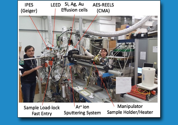
IPES
- Working pressure ~10-11 mbar
- Iodine / SrF2 Geiger- Müller detector2 : photon resolution ΔE=0.25 eV a 9.5eV;
- Collimated, BaO cathode based electron beam gun ΔE=0.3 eV);
- LEED optics, e-- (0-0.5) KeV;
- Camera for data diffraction pattern acquisition.
-
Preparation chamber
- Working pressure ~10-10 mbar
- Si, Ag, Au solid effusion cells (two of them can be exchanged without breaking the UHV conditions)
- Ag, Zn- effusion cells- Capping Layer ;
- DC direct sample heating (RT-1200 °C) and Indirect heating (RT-450 °C ) systems;
- Quartz Microbalance;
- sputtering system Ar+ Ion +;
- O2 Gas-line2;
- AES/SE/REELS spectroscopies; double-pass CMA, e- (HV = 0-5 KeV) ΔE=1.2%PE (UPS/ESCA); ΔE=1.2%Ekin eV (AES);
- Air-vacuum Fast Load-lock Sample Transfer System
AVAILABLE TECHNIQUES
- Ultra-High Vacuum (UHV) System for Surface Science Investigations
- IPES/LEED/AES/SE/REELS systems;
- Chemical composition chemical bonding at surface; work function, molecules hybridization and valence orbitals investigation
- Diffraction pattern from low-e-;
- Analysis of samples in the presence of a gases (O and other);
- Heating of samples from RT to 1200 °C during analysis;
- Clean Semiconductor (SC), Metal (M)-Surfaces reconstruction
- Epitaxial growth SC/SC, SC/Metal/SC:
- Homo- and Hetero-structures growth: 1D, 2D and 3D Materials.
SAMPLES
-
Sample lateral dimensions: 10 x 5 mm (ideal), 3 x 3 mm (minimal), 10 x 10 mm (maximal);
-
Sample thickness: ideally up to 2 mm (thicker and/or smaller samples also feasible).
USED FOR
-
Fundamental Surface Science study
-
Artificial Atomic Epitaxial Growth;
-
Discovery of new 1D, 2D and 3D epitaxial SC/SC; M/SC for micro-nanoelectronics and solar cells purposes;
-
Semiconductor/ Microelectronics;
-
Microcircuits;
-
Ultra-thin Films;
-
Samples Cleaning;
-
Thin-film Stability;
-
Barrier Layers;
-
Lubrication;
-
Chemical Industry;
-
Coatings/Catalysis.
CASE STUDIES
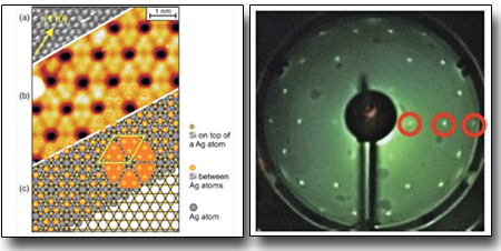
(4✕4) Silicene on Ag(111)1✕1 Because of its unique physical properties, graphene, a 2D honeycomb arrangement of carbon atoms, has attracted tremendous attention. Silicene, the graphene equivalent for silicon, could follow this trend, opening new perspectives for applications, especially due to its compatibility with Si-based electronics. Silicene has been theoretically predicted as a buckled honeycomb arrangement of Si atoms and having an electronic dispersion resembling that of relativistic Dirac fermions. Here we provide compelling evidence, from both structural and electronic properties, for the synthesis of epitaxial silicene sheets on a silver (111) substrate, through the combination of scanning tunneling microscopy and angular-resolved photoemission spectroscopy in conjunction with calculations based on density functional theory.
P. Vogt et al., Phys. Rev. Lett. 108, 155501 (2012)
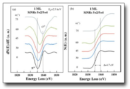
Silicene nanoribbons on Ag(110) Silicene nanoribbons grown on a silver (110) substrate have been studied by reflection electron energy loss spectroscopy as a function of the electron beam incidence angle a. The spectra, taken at the Si K absorption edge (1.840 KeV), reveal the presence of two distinct loss structures attributed to transitions 1s→p* and 1s→s*, according to their intensity dependence on a. Such behavior, when compared to graphite, attests the sp2-like hybridization of the silicon valence orbitals in the silicene nanoribbons as is, indeed, for carbon atomic bonds of graphene.
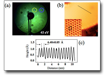
P. De Padova, et al., App. Phys. Lett. 98, 081909 (2011)(a) REELS spectra at the Si K-edge from the 5×2/5×4 SiNR grating collected in derivative mode a and numerically integrated (b) The energy loss spectra are referred to the primary elastic peak, EP=2.5 KeV. LEED patterns for ~10 MLs of silicon deposited onto the Si(111)√3–Ag surface at ~ 200 °C, yellow circle: (1/3,1/3) order spot of the Ag √3×√3 reconstruction; blue circle: silicon integer order spot (a). Empty- and filled-state STM constant-current images, measured at 77 K from ~ 5 MLs of silicon deposited onto Si(111)√3–Ag surface at ~ 200 °C: (b) 15×15 nm2 (50 pA and -1.0 V) and its inset 5×5 nm2, (50 pA and 0.4 V) at atomic resolution; √3×√3-Si unit cell is drawn. (c) is the line profile of the black line of (b). Multilayer Silicene on Ag(111) We report new findings on multilayer silicene grown on Si(111) √3×√3 R30°–Ag template, after the recent first compelling experimental evidence of its synthesis. Low-energy electron diffraction, reflection high-energy electron diffraction, and energy-dispersive grazing incidence X-ray diffraction measurements were performed to show up the fingerprints of √3×√3 multilayer silicene. Angle-resolved photoemission spectroscopy displayed new features in the second surface Brillouin zone, attributed to the multilayer silicene on Si(111) √3×√3 R30°–Ag. Band-structure dispersion theoretical calculations performed on a model of three honeycomb stacked layers, silicene grown on Si(111)√3×√3 R30°–Ag surface confirm the experimental results.
P. De Padova, et al., Materials 12,2258,(2019) doi:10.3390/ma12142258
 Italiano (Italia)
  English (UK)