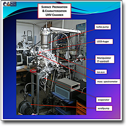
Low Electron Energy Diffraction (LEED) is a surface-sensitive spectroscopic technique that allows evaluating the long-range order (typical coherence length of 100 Å) of atoms at the topmost layers (few Å) of solid samples. In the same experimental instrument the retarding field analyzer technique allows extension to Auger Electron Spectroscopy (AES) as well as Electron Energy Loss Spectroscopy (EELS), making possible to quantitatively evaluate the elemental composition at the parts per thousand range, chemical state and electronic state of the elements that exist within a material. AES and EELS spectra are obtained by impinging the sample with the same LEED electron beam, while simultaneously measuring the kinetic energy and number of electrons that escape from the top 0 to 10 nm of the material being analyzed.
In-situ preparation of clean and ordered surfaces at atomic level by noble gas sputtering and thermal annealing in ultra high vacuum (UHV).
Morphological and elemental analysis of surface and interfaces by LEED/AES-EELS techniques.
Ultrathin film growth by Chemical Vapor Deposition (CVD) is also possible by monitoring the overlayer thickness with a sub-monolayer grade of precision.
TECHNICAL SPECIFICATIONS
- Working pressure: 10-11 mbar – 10-5 mbar (Ar-sputtering)
- Working temperatures: RT – 1000 °CC (Annealing)
- LEED/ AES- EELS
- Working pressure: 10-11 mbar – 10-8 mbar (filamento del cannone elettronico a cristallo singolo di LaB6)
- Primary energy 0-1000 eV (LEED), 0-3000 eV (EELS-AES)
- Spot size: << 1 mm @1 μA & 100 eV
- A z-retraction mechanism allows the optics to be moved into or withdrawn from a restricted working area. Z-travel of 100 mm
- Sample in vertical position, sample biasing, sample rotation:
UHV manipulator enables 4 degrees of freedom (x, y, z,θ)
AVAILABLE TECHNIQUES
- UHV standard Surface cleaning techniques (Ar-sputtering and Thermal Annealing)
- Ultrathin film growth by Chemical Vapor Deposition (CVD)
- LEED (four grids setup, back view)
- AES-EELS (retarding field technique, derivative mode)
SAMPLE
-
Sample lateral dimensions: 5mm x 5 mm
-
Sufficient electrical conductivity of samples needed to avoid charging
-
Mechanical integrity of samples needed because they are measured in vertical position (powder samples should be in a form of pellets or pressed into soft metal foil or mesh)
-
No availability for liquid samples
USE FOR
- Ultra-thin Films Growth
- Surface Cleaning
- Chemical Physics Characterization of Surfaces and Interfaces
- Pre-qualifying activity for experiments RomaTre LaSEC at the laboratory (https://app.scienze.uniroma3.it/research/lines/3) and large scale facilities
 Italiano (Italia)
  English (UK)