Scanning Probe Microscopy (AFM, SNOM) and Angle Resolved (UPS)
Antonio Cricenti -
Laboratory Nanospectroscopy
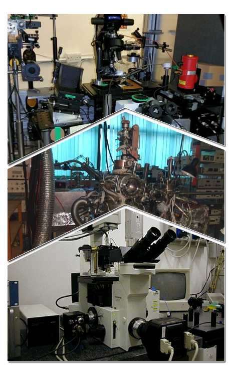
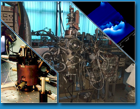
ISM-CNR is a leader institution in the field of Scanning Probe Microscopy. For more than thirty years, ISM researchers have designed, constructed and used Atomic Force (AFM), Scanning Near-field Optical (SNOM), and Scanning Tunneling (STM) Microscopes for material science and biology applications. This activity has also produced several patents and high-level scientific publications. SNOM and AFM are well established techniques which, through the controlled scanning of a suitable sharp probe (a tapered optical fibre or a very sharp Si/Si3N4 tip respectively) above the sample surface, allow to collect topography images with resolution in the nanometer scale and, at the same time, to map other interesting properties of the samples. These “collateral” properties can be, typically, lateral friction/phase lag images when using AFM as well as reflectivity, transmittivity or fluorescence properties of the samples with a resolution well below the diffraction limit when employing a SNOM. Furthermore, both the techniques can be operated in air, in vacuum or in a suitable liquid environment (e.g. the physiological solution used to grow cells cultures). This latter, in particular, is an invaluable advantage when studying living systems.
ARUPS chamber is used for characterizing semiconductor/metal surface in UHV with angle resolved photoemission bands, Auger and XPS. Real metallic substrates for biological purpose are also chemically characterized.
All the AFM-SNOM instruments can be run in different modes of operations (contact, shear or tapping mode) and, in particular, the SNOM can employ different set-ups (tip illumination, tip collection or illumination/collection modes) optimized to match specific experimental demands. Local internal phoemission , reflectance, transmission, fluorescence can be performed in the UV-IR range (lambda 0.4-10 micron). Any kind of sample can be observed within a range from few nm to half millimiter with chemical sensitivity.
Angle Resolved Ulraviolet Photoelectron Spectroscopy (ARUPS) is a surface-sensitive quantitative spectroscopic technique that measures the energy of emitted electrons and their emission angle and, consequently the k-vector information. Spectra are obtained by irradiating a material with a beam of UV-rays (20-40 eV) while simultaneously measuring the number of electrons with a certain kinetic energy that escape from the top 0 to 10 nm of the material being analyzed.
Auger and XPS angle resolved measures the elemental composition at the parts per thousand range of materials and are obtained by irradiating a material with a beam of electrons (Auger) or X-rays (XPS)while simultaneously measuring the kinetic energy and number of electrons at any emitting angle, thus being more sensible to the surface or to the bulk.
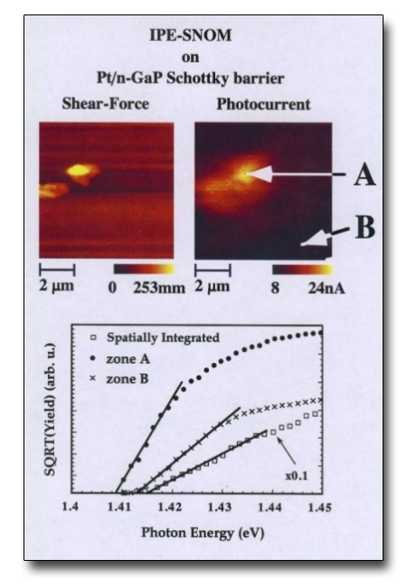
Local Internal Photoemission
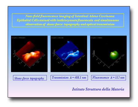
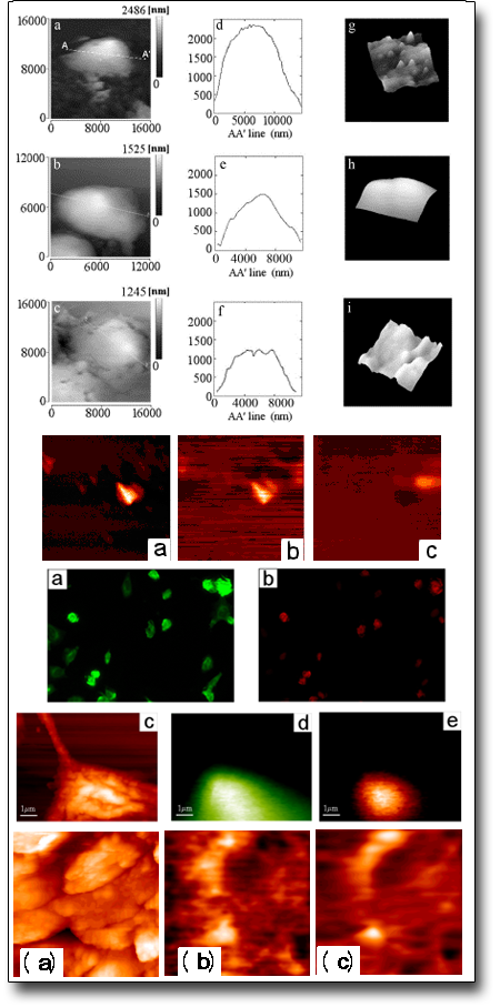
Transmission and fluorescence SNOM
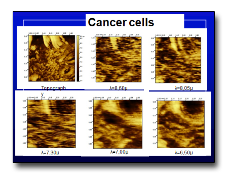
Cancer cells reflectance by IR-SNOM
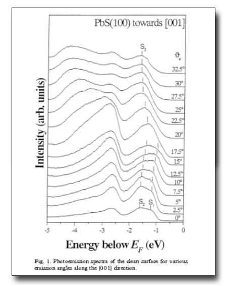
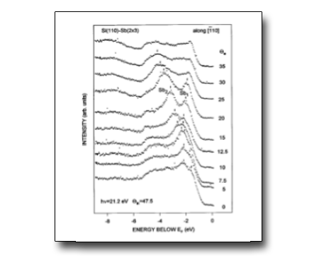
Angular photoemission spectra
TECHNICAL SPECIFICATIONS
- AFM
Range up to 200 micron- Possibility to working in liquid
- Metals, semiconductors, magnetic and biological samples
- Petri cell
- Working in liquid
- SNOM
Range up to 400 micron- tip illumination, tip collection or illumination/collection modes optimized to match specific experimental demands.
- Local internal photoemission , reflectance, transmission, fluorescence in the UV-IR range (lambda 0.4-10 micron)
- ARUPS
ARUPS Working temperatures: 120 – 1000 K- Sample in vertical position, sample biasing, sample rotation
- UHV manipulator enable standard UHV ARUPS, Auger and XPS
AVAILABLE TECHNIQUES
- AFM
- Contact, friction, non contact, tapping mode
- Imaging and Mapping of the topography and chemical composition
- SNOM
Scan up to 400 microns- Imaging and Mapping of the topography and chemical composition of samples
- Local internal photoemission , reflectance, transmission, fluorescence
- ARUPS
- Valence band dispersion with 50 meV energy resolution
- Auger survey in the energy range 5-3000 V
- XPS survey in the energy range 5-600 V
- Chemical composition chemical bonding of the surface with resolution of 0.1-0.5 eV
SAMPLE
-
No sample limitation for AFM and SNOM
-
ARUPS: Sample lateral dimensions: 10 x 5 mm
-
Sufficient electrical conductivity of samples needed to avoid charging
-
Time for loading the sample and its transfer to measuring position is 30 min
-
Cleaning by ion-bombardment and annealing.
-
Metal-semiconductor evaporation of thin films
USE FOR
-
AFM e SNOM
-
Material science and biological samples
-
-
ARUPS
-
Clean Semiconductor/ Metal surfaces
-
CASE STUDIES
Scanning Probe Microscopy in Material Science and Biology
A review of the activity of scanning probe microscopy at our Institute is presented, going from instrumentation to software development of Atomic Force Microscopy (AFM) and Scanning Near-field Optical Microscopy (SNOM). Some of the most important experiments in material science and biology performed by our group through the years with these SPM techniques will be presented. Finally, infrared applications by coupling a SNOM with a Free Electron Laser will also be presented.
See: Antonio Cricenti et al. J.Appl.D 44, 464008 (2011)
Electronic and optical properties of group IV two‐dimensional materials Electronic evidence of asymmetry in the Si(111)√3×√3−Ag structure
Si(110)2x3-Sb surface studied with Angle-resolved photoemission.
See: O.Pulci et al. Phys. St. Sol. A207, 291 (2010)
I.Matsuda et al. Phys. Rev. B68, 085407 (2003)
A.Cricenti et al. J. Vac. Sci. Technol. A15, 133 (1997) Italiano (Italia)
  English (UK)