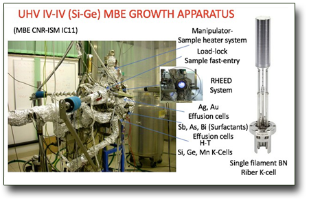
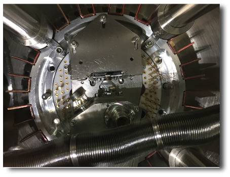
TECHNICAL SPECIFICATIONS
- Working pressure ~10-11-11 mbar
-
Si(C-BN-1400 °C), Ge(BN-1200 °C, Mn(BN-1200 °C) K-cells; Si (flux=0.04 Å/min); Ge (flux=0.16 Å/min);
-
Sb, As, Bi- Surfactants effusion cells;
-
Ag, Au- Capping Layer effusion cells;
-
DC direct sample heating (RT-1200 °C) and Indirect heating (RT-450 °C ) systems;
-
Air-vacuum Fast Load-lock Sample Transfer System;
-
Variable e- HV (0-15 KeV) for RHEED system;
-
Hi-Speed Camera for real-time data diffraction acquisition (Image-software-MAC).
AVAILABLE TECHNIQUES
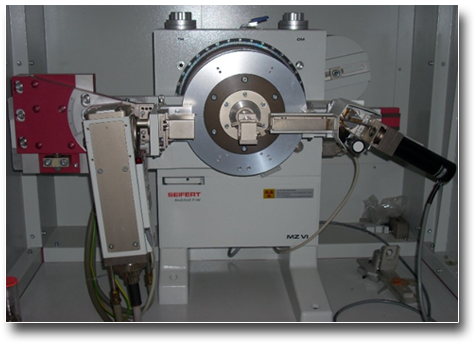
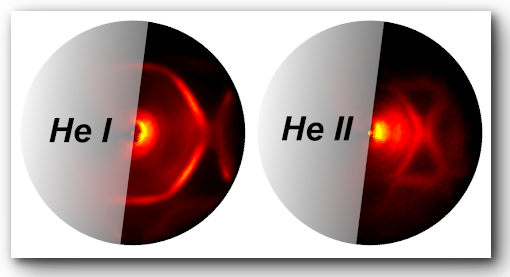
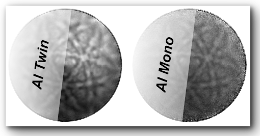
- RHEED Ultra-High Vacuum (UHV) System for Surface Science Investigations;
- Cleaning Semiconductor (SC), Metal (M)-Surfaces reconstruction;
- Epitaxial growth SC/SC, SC/Metal/SC;
- Homo- and Hetero-structures growth: 1D, 2D and 3D Materials.
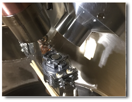
SAMPLES
-
Sample lateral dimensions: 10 x 5 mm (ideal), 3 x 3 mm (minimal), 10 x 10 mm (maximal);
-
Sample thickness: ideally up to 2 mm (thicker and/or smaller samples also feasible).
USED FOR
-
Fundamental Surface Science study;
-
Artificial Atomic Epitaxial Growth;;
-
Discovery of new 1D, 2D and 3D epitaxial SC/SC; M/SC for micro-nanoelectronics and solar cells purposes;
-
Semiconductors for Microelectronics;
-
Microcircuits;
-
Ultra-thin Films;
-
Samples Cleaning;
-
Thin-film Stability;
-
Barrier Layers;
-
Lubrication;
-
Chemical Industry;
-
Coatings/Catalysis.
CASE STUDIES
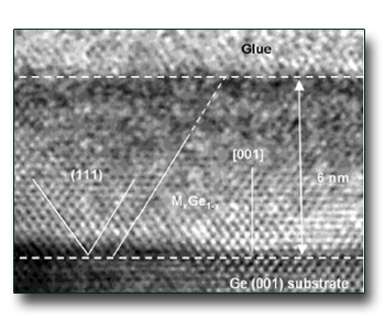
Cross-sectional high-resolution transmission electron microscopy (HRTEM) image of a Mn0.06Ge0.94 film grown on a Ge(001)2✕1 substrate held at 520 K0.06Ge0.94 on Ge(001)2✕1
The structural, electronic, and magnetic properties of the Mn0.06Ge0.94 diluted magnetic semiconductor0.06Ge0.94, grown at 520 K by molecular-beam epitaxy on Ge(001)2✕1, have been investigated. Diluted and highly ordered alloys, containing Mn5Ge3 nanocrystals5Ge3. The valence band photoelectron spectrum of Mn0.06Ge0.94 shows a feature located at −4.2 eV below the Fermi level, which is the fingerprint of substitutional Mn atoms in the Ge matrix. Magnetization measurements show the presence of a paramagnetic component due to substitutional Mn atoms and of a ferromagnetic like component due to Mn5Ge3. The Mn L2,3 x-ray absorption spectrum of this polyphase film shows no marked multiplet structure, but a bandlike character.
See: P. De Padova, et al., Phys. Rev. B 77, 045203 (2008).
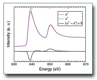
Spettri di assorbimento a raggi-X di L2,3 di Mn misurati per polarizzazione circolare della luce destra [σ+ (linea rossa)] and sinistra [σ− (blue dashed line)] e il corrispondente segnale XMCD (σ+ − σ−) (linea nera).
See: W. Ndiaye et al., Phys. Rev. B 91, 125118 (2015).
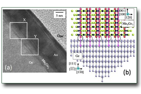
Mn5Ge3 film on Ge(111)
An investigation of the structural, magnetic and electronic properties of≈3 nm thick Mn5Ge3 grown on a Ge(111)-c(2✕8) reconstructed surface is reported. High resolution transmission electron microscopy and selected area electron diffraction give evidence of 2.2% in-plane compressive strain between the Mn5Ge3 and the Ge substrate. Magneto optical Kerr effect measurements show that the films are ferromagnetic with a Curie temperature of ≈325 K. The analysis of Ge 3d core level photoelectron spectra of the Mn5Ge3 allows determining an upper limit of 76 meV for the Ge 3d5/2 core-hole lifetime broadening Ge 3d5/2. The Ge 3d3/2 core-hole lifetime broadening is found to be 15 meV larger than that of the Ge 3d5/2 core hole3/2 5/2, because of the existence of a Coster–Kronig decay channel due to the metallic character of Mn55Ge3.
See: P. De Padova, et al., Phys. Rev. B 77, 045203 (2008).
 English (UK)
  Italiano (Italia)