Diamond exhibits intrinsic semiconducting characteristics that make it the ideal material for fabrication of high-frequency high-power solid state devices.
Hydrogen on diamond surface forms a dipole that turns the diamond electrical insulating behavior into a p-type conductor. The peculiar nature of the H-induced charge transport is characteristic of a quasi 2D hole gas transport produced in a 3D semi-conductor that enables the development of technologically-simple electronic devices characterized by very high performance. Indeed, p-type conducting channels led to develop surface-channel MESFETs with an operating frequency up to 120 GHz. The hydrogenated diamond system can also be used for producing high-performance gas and bio-electrochemical sensors.
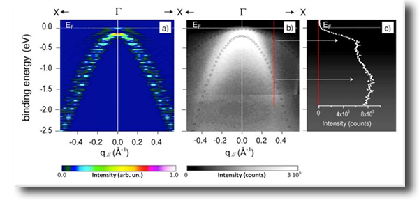
The full exploitation for commercial appli-cations relies upon the understanding at a microscopic level of the basic mechanism enhancing the surface conductivity, strictly depending to details of the electronic structure that remains up to now elusive.
Staff: S. Iacobucci, P. Alippi, A. Bellucci, M. Girolami, D.M. Trucchi
 English (UK)
  Italiano (Italia)