Ore 15.00 Saluto del Direttore CNR-ISM - Dr. Antonio Cricenti
Ore 15.05 Saluto del Presidente del CNR - Prof. Maria Chiara Carrozza
Ore 15.10 Il Premio PRISM - Prof. Aldo Di Carlo
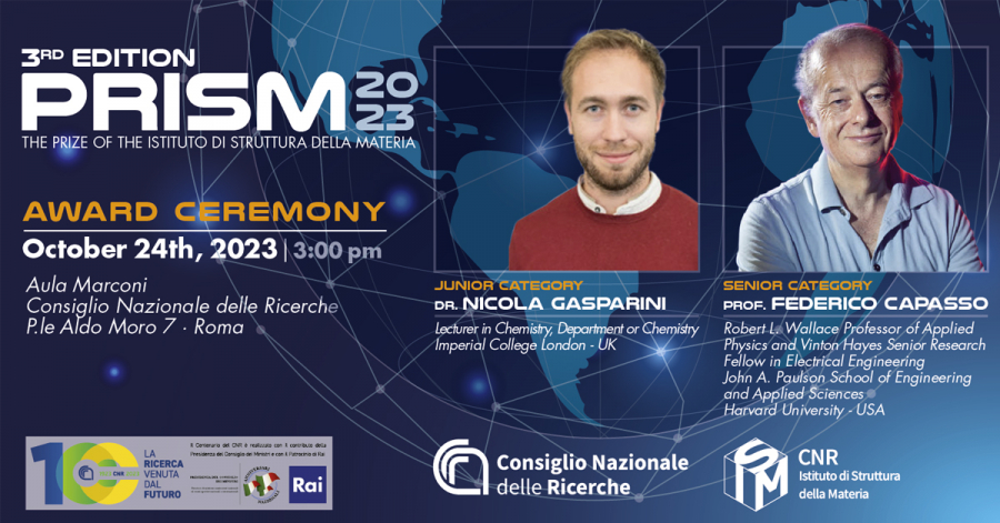
Ore 15:15 Dr. Nicola Gasparini, vincitore categoria PRISM Junior - Lecturer in Chemistry, Department of Chemistry, Imperial College London - UK
Ore 15:45 Prof. Federico Capasso, vincitore categoria PRISM Senior - Robert L. Wallace Professor of Applied Physics and Vinton Hayes Senior Research Fellow in Electrical Engineering, John A. Paulson School of Engineering and Applied Sciences, Harvard University - USA
Ore 16.15 Premiazione
Ore 16.30 Conclusione
Abstract
From UV to Near-Infrared light detection: next generation photodetectors for imaging and biometric applications
Nicola Gasparini
Department of Chemistry, Imperial College London - UK
The current success of organic semiconductor technology is mainly driven by the development of organic light-emitting diodes (OLED), which are now routinely employed in display technologies. In the last decade, however, organic photovoltaics (OPV), leveraging the impressive improvement in device efficiency and stability, have gradually moved from a lab curiosity to a niche market. Their recent success has coincided with the rapid development of effective replacements for the fullerene-based materials that have been prevalent as electron acceptor materials until recently; namely the small molecule nonfullerene acceptors (NFAs). This relatively new class of materials offer a number of opportunities to develop new areas of research. Between those, organic photodetector (OPD), a technology based on organic photodiodes and thus closely related to OPV, is one of the most exciting. Recent efforts in the field of OPD have been focused on extending broadband detection into the near-infrared (NIR) region. The early absorption cut-off of solution processed organic semiconductors presents a challenge in achieving NIR detection, however, careful tuning of their chemical structures can help extend OPD responsivity into the infrared window. Here, we discuss how to design donor:acceptor blends and control charge carrier recombination in organic photodetectors for NIR light-to-current conversion for high efficiency and stable devices.
Designer Materials: from Quantum Cascade Lasers to Flat Optics
Federico Capasso
John A. Paulson School of Engineering and Applied Sciences - Harvard University - USA
I will discuss the work I carried out with my groups at two institutions, Bell Laboratories (1977-2002) and at Harvard University(2003-present). I arrived at Bell Laboratories at the dawn of the new area of artificially structured semiconductor materials, enabled by the invention of a new epitaxial crystal growth technique, Molecular Beam Epitaxy (MBE), pioneered by my colleague Alfred Y. Cho in the late sixties. MBE basically consists of the equivalent of spray-painting materials one atomic layer at a time in a high-vacuum chamber, to achieve thin films of semiconductors with unprecedented control of thickness (down to one monolayer) and composition. In this way quantum wells, superlattices and a wide range of nanostructured materials could be grown. I realized that I could design the band structure of these manmade materials to endow them with electronic and optical properties not existing in the bulk constituent materials (band structure engineering) and which I could use for a new class of transistors, photodetector, lasers, and quantum devices.1 The Quantum Cascade Laser (QCL) (1994) was the most important fruit of this research.2 Its key feature is that its operating wavelength can be designed, using the same combination of materials, to cover the entire spectral range from 3 µm to ~ 20 µm, known as the mid-infrared or molecular fingerprint region because most molecules have there their telltale absorption features. QCLs have now become the most widely used laser in this spectral region in a wide range of scientific, industrial, and military applications and by using them as pumps for molecular gases they have led to a new class of compact high performance THz lasers operating at room temperature.
While at Harvard University I became interested in the rapidly expanding field of metamaterials. What caught my attention was that such bulk materials, while very interesting from the point of view of the physics, were inherently difficult to fabricate at optical frequencies for the obvious reason that the standard lithography-based processing is not applicable for structuring the bulk at the (sub) wavelength scale. I made the decision then to explore structuring surfaces at the sub-wavelength scale to explore 2D_metamaterial (metasurfaces), where I saw not only the opportunity to revisit some established laws of optics and discover new phenomena, but also to design a new class of diffractive optical components made of metaatoms, the dispersion of which could be tailored at will. This was the beginning of the field now known as meatoptics or flat optics. Our fist success came with the generalization of Snell’s law3 and its use in designing spherical aberration-free lenses (metalenses)4, later followed by the demonstration of a new kind of polarization optics based on shape birefringence which led to a new polarization sensitive camera.5 The significance of metaoptics is twofold: (1) the emergence of a new class of basically flat components, much easier to align and stack with the underlying sensor, and in the case of imaging, with much easier control of aberrations, while minimizing the number of lenses; (2) technological, in that they can be mass produced with deep-UV lithography used for semiconductor chip manufacturing. Thus, the foundries that manufacture the latter can now do the same for the optics. The implications of this new paradigm are major and will impact consumer electronics in areas like cell phones, laptops and automotive, since now the complete camera module (electronics plus optics) will be manufactured with CMOs compatible processing. Based on this vision I started in 2017 with my former graduate student Rob Devlin, a company Metalenz, www.metalenz.com to pursue such market opportunities.
1. F. Capasso, Science 235,172 (1987)
2. J. Faist, F. Capasso, D. L. Sivco, C Sirtori. A.L. Hutchinson, A. Y. Cho Science 264, 553 (1994)
3. N. Yu, P. Genevet, M. A. Kats, F. Aieta, J-P. Tetienne, F. Capasso, Z. Gaburro, Science 334,333 (2011)
4. M. Khorasaninejad, W. T. Chen, R. C. Devlin, J. Oh, A. Y. Zhu, and F. Capasso, Science 352 1190 (2016)
5. N. A. Rubin, G. D'Aversa, P. Chevalier, Z. Shi, W-T Chen, F. Capasso. Science, 365, 43 (2020)
 Italiano (Italia)
  English (UK)