Germanium, one of the first semiconductors historically employed for electronic devices, has recently re-gained attention in the field of mid-infrared imaging technique, where femtosecond laser can be used for optimal polishing of Ge optical substrates.
CNR-ISM, in collaboration with the University of Tlemcen (Algeria), has developed a theoretical model able to dynamically track the evolution of high-spatial-frequency laser-induced periodic nanostructures in Germanium thin films.
The model, named as TTM++, uses a doubly extended two-temperature model coupled with a carrier density rate equation and a generalized plasmonic model, and can be applied to all bandgap materials. In addition, the feasibility of a novel low-fluence irradiation method (“burst” mode) is applied to Germanium for the first time, enhancing the control on the laser-induced surface modification while minimizing thermal damage.
Wednesday, 02 April 2025 09:31
Dynamic evolution of high spatial frequency femtosecond laser-induced periodic surface nanostructures on Germanium thin films - New article
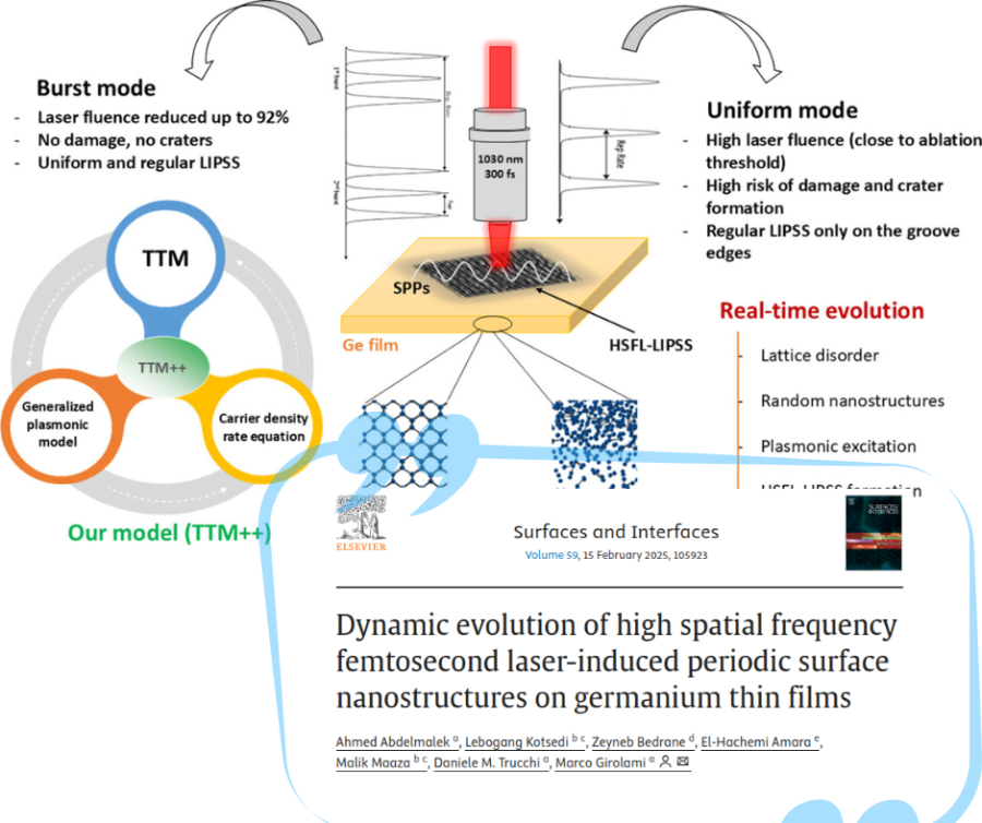
The paper presents a comprehensive theoretical study of the mechanisms underlying the formation of high-spatial-frequency periodic nanostructures (HSFL-LIPSS) induced by 300 fs laser pulses on crystalline Germanium thin films, allowing to identify the physical phenomena that occur in the very early stages of the process.
In particular, HSFL-LIPSS are due to ultrafast processes such as non-thermal melting, in which the material lattice remains cold despite the change of state.
Article published in Surfaces and Interfaces.
Published in
Publications